Seeing the Nanoworld
Seeing the Nanoworld
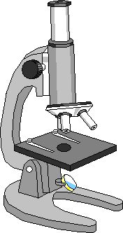
 Nanotechnology is the science and engineering of small things. Nanostructures can be as small as 1/1000th the diameter of a human hair! Wow that’s small! A typical question we are often asked is “If nanoscale objects are so small (1 to a few hundred nm) then how can you see them?” To see nanostructures it takes some pretty sophisticated instruments To answer that question we need to explore how we magnify objects. Let’s begin with the most common way we enlarge our view of an object – magnifiers (hand lens) and optical microscopes.
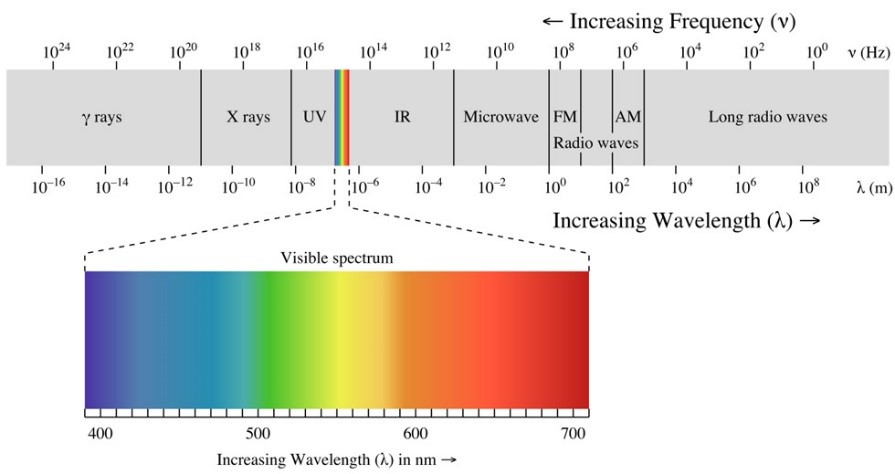
When we think about magnification we often think of optical (light) microscopes. These instruments focus visible light through “lenses” to make a magnified image. They work essentially like a magnifying glass. But even with the most powerful optical microscope, one problem remains—light waves are “big”, at least on the scale of nanostructures.As the resolution power of optical instruments is limited to about half of the wavelength of visible light (390-700nm), they can only reveal features down to ~250 nm.
 When we talk about seeing small structures, it is important to distinguish between “resolution” and “magnification”. We can enlarge (magnify) an image (e.g. a picture) as much as we want - make it as big as a poster on your wall - but that does not make the image any sharper or increase our ability to resolve small structures – i.e. to have sharp edges and to distinguish separately closely spaced objects. Enlarging a picture too big just gives you a fuzzy big picture; that is called “empty magnification” and it does us little good. What is important is the ability to sharply see structures that are close to each other. This is called resolution and is the most important property of any microscope.
Optical microscopes give us a top-down, flat, "airplane" view of the surface. It is difficult to learn much about 3-D objects with a high powered optical microscope because they have very low "depth of field"- i.e. only objects at a certain, very narrow height will be in focus. For a high magnification optical microscope, this "depth of field" can be less than 1 micro meter- anything taller than 1 micrometer is out of focus and blurry. With a super high quality optical microscope, we see and resolve structures down to about 250 nm. That still leaves a lot of nanoscale objects and features that we can’t see. For those, we need an electron microscope.
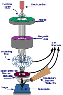
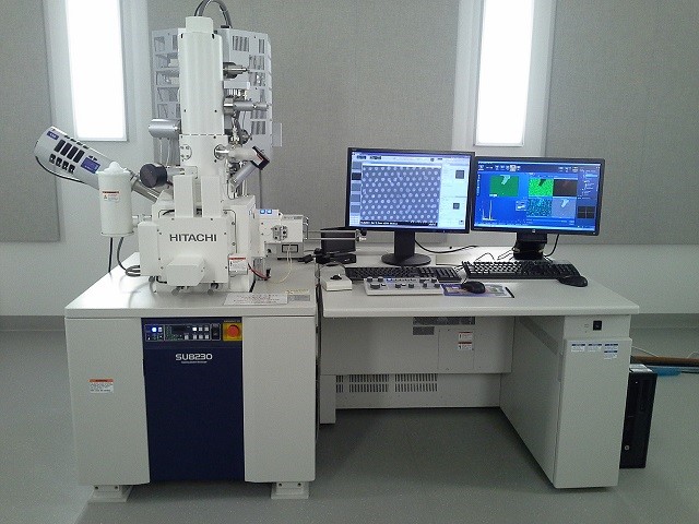 Electron Microscopes (EM) use electron beams instead of visible light, enabling resolution of features down to a nanometer. Several different types of EMs exist, including Scanning Electron Microscopes(SEM), Transmission Electron Microscopes (TEM), and Scanning Transmission Electron Microscopes (STEM). EMs use a beam of high energy electrons to probe the sample. Electrons do not suffer the same resolution limits that light does, so we can “see” features as small as 0.1 nm. This is the size of an individual atom. Electronic signal processing is used to create a picture of what the sample would look like if we could see it. While electron microscopy offers finer resolution of features than does optical microscopy, it requires vacuum conditions in order to maintain a focused electron beam. This makes electron microscopy inconvenient for examining many biological samples, which must first be preserved and coated with layers of metal atoms. Another advantage of electron microscopes is that they have both high magnification and high depth of field. We can see objects as in apparent three dimensions. This is again due to the short "wavelength" of electrons. You may have seen some really "monster" like pictures of bugs that highlight the imaging capabilities of the scanning electron microscope. High quality electron microscopes can cost from $250,000 to $1,000,000! They are one of the most useful instruments in our laboratories.

Scanning Probe Microscopes (SPM) of various types trace surface features by movement of a very fine pointed tip mounted on a flexible arm across a surface.SPM enables resolution of features down to ~1 nm in height, allowing imaging of single atoms under ideal conditions. Scanning Tunneling Microscopes (STM) measure current (i.e., electron flow) between the probe tip and sample, essentially acting like a tiny voltmeter. This method requires that the sample be electrically conductive. Atomic Force Microscopes (AFM - sometimes call Scanning Force Microscopes) measure interaction forces between probe tip and sample, providing information on the mechanical properties of surfaces. They can measure forces of 10-9 Newton. (For comparison, the force exerted by an apple is ~1 N.) AFMs are widely used to measure surface topography of many types of sample and do not require special conditions such as conductive surfaces or vacuum.
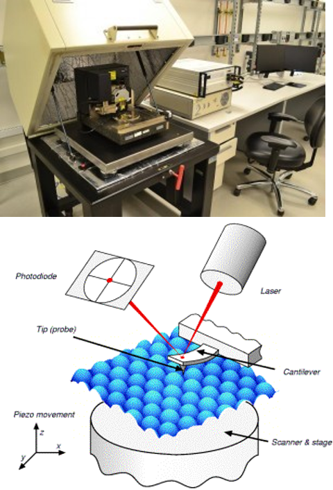
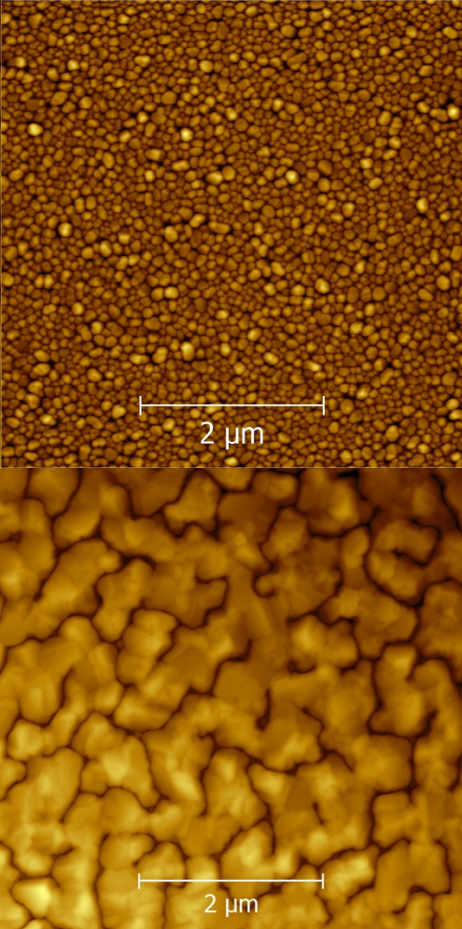
SPMs and particularly AFMs basically see things by touching. Imagine you have your right hand in a dark box with a mystery object and you are trying to figure out what the object is, without looking. One systematic way to do this would be to touch every point on a grid, say 30 points wide and 30 points deep, covering the entire floor of the box. Imagine that with your left hand, you record the “height” (or any other physical property) at each grid point on a piece of graph paper. You could then make a 3-D graph surface, or a 2-D plot with colors indicating height. After touching and recording 900 points, you would have a “picture” of the object. That is exactly what an atomic force microscope does, except the AFM uses a very fine point instead of a finger, and is built on a mechanism that can reproducibly move the tip less than 0.1 nm between points. Scanning probe microscopes can actually ‘feel” the bumps due to individual atoms and molecules!
Want to explore these exciting instruments? Check out these online resources:
My Scope virtual step by step SEM simulator – developed by the Australian Microscopy and Microanalysis Research Facility and FEI. This interactive application allows you to “operate” and SEM.
Molecular Expressions Virtual Electron Microscopy – developed by Florida State University. The interactive tutorials allow exploration of various aspects of virtual Scanning Electron Microscopy.
The Virtual Microscope – developed by the University of Illinois Champagne Urbana. This site explores Environmental SEM, AFM, and Fluorescence Light Microscope.
Amazing Creatures with Nanoscale Features- developed by our colleagues at Penn State's Center for Nanotechnology Education and Utilization. This animation is an introduction to microscopy, scale, and applications of nanoscale properties.
UVA Virtual Lab – developed by the University of Virginia. Virtual interaction with a variety of scientific instruments including AFM, SEM, and STM.
Discovery Education Virtual Electron Microscope – developed by the Discovery Channel. Match SEM images with the actual sample.
Remotely Accessible Instruments for Nanotechnology (RAIN) – developed by Pennsylvania State University. Provides remote access to microscopes located at 10 colleges and universities.

