
NNCI Image Contest 2019 - Unique
Most Unique Capability
This category celebrates the unique capabilities each site of the NNCI has on offer. Click on the image you think captures the most unique capability of the NNCI in order to vote for it. You may vote for only one image in this category.
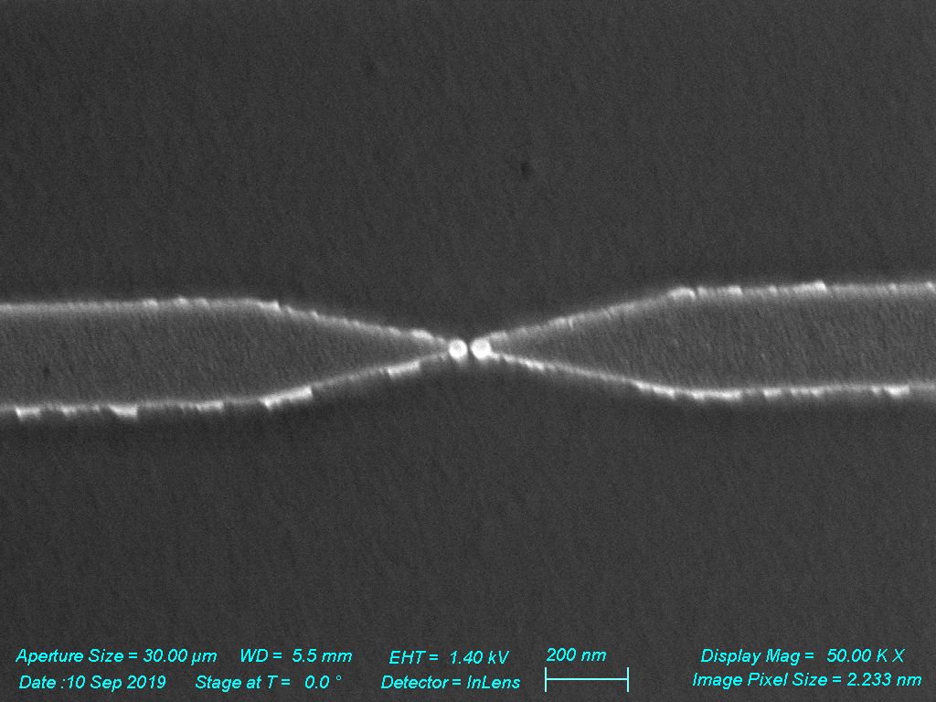
Dot on Tip
Artists: Chulmin Choi, Roswell Biotechnologies, and Maribel Montero, Nano3 Staff, University of California-San Diego
NNCI Site: SDNI
Tool: Zeiss Sigma 500 Scanning Electron Microscope
This SEM image shows two Au nanodots (40 nm diameter each) deposited on the tips of two electrodes separated by a 12 nm gap. Both the tips of electrodes and the Au nanodots are written by electron beam lithography with alignment accuracy better than 5nm. The device enables measurements of tunneling currents through a single molecule such as a double-strand DNA molecule positioned at the 12nm gap.
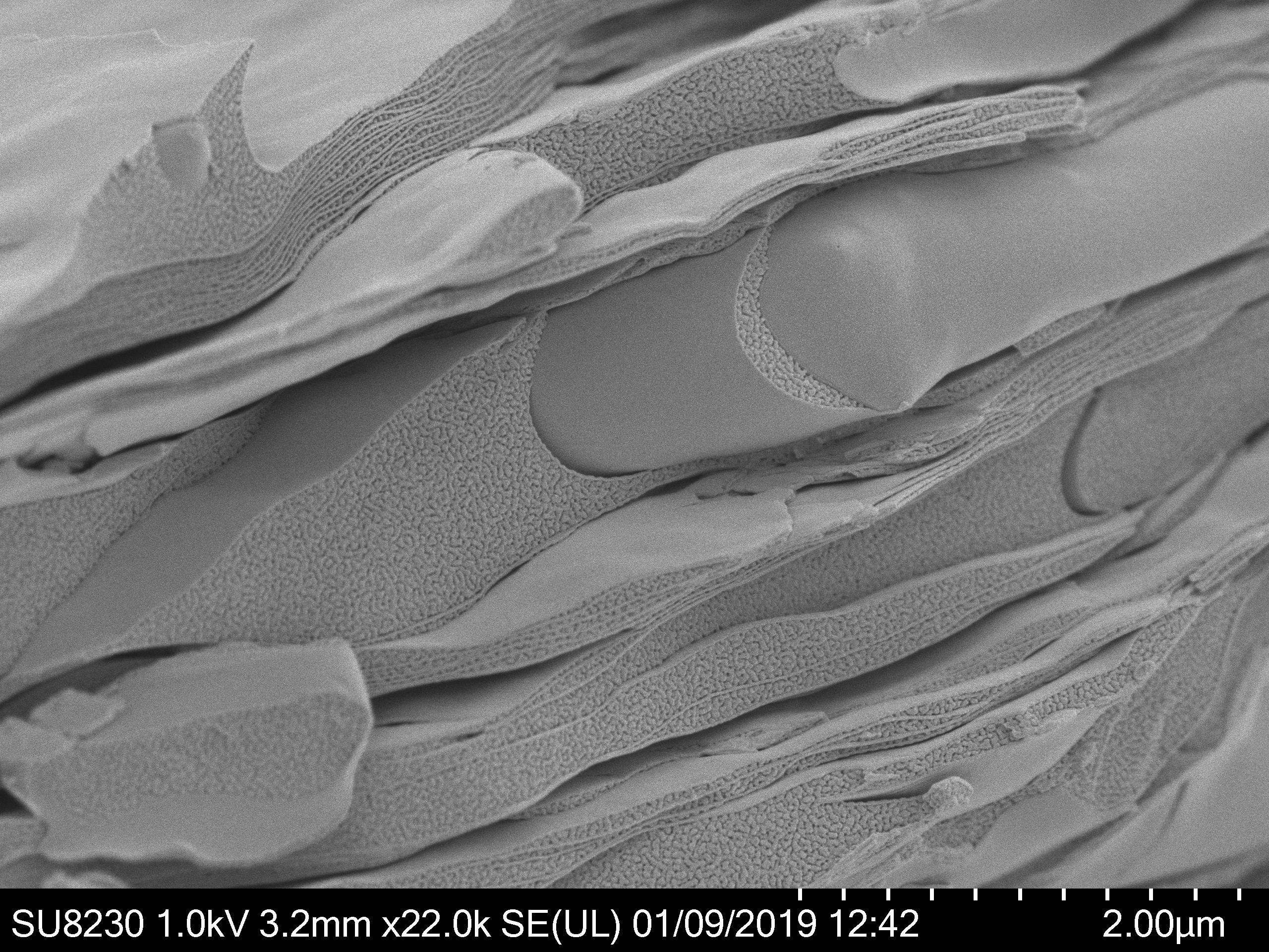
Cryo-SEM of Body Lotion
Artists: Hanseung Lee and Chris Frethem, Staff Scientists, University of Minnesota
NNCI Site: MINIC
Tool: Hitachi FE-SEM SU8230
This is an example of MINIC’s cryoSEM capabilities. The sample is a body lotion (CeraVe®, personal care product), advertised as having multivesicular emulsion technology. The image shows emulsion droplets with lamellar structure. The specimen was frozen with a high pressure freezer, sublimed at -100 C for 5 minutes, and then sputter coated with Pt for 7.5 nm.
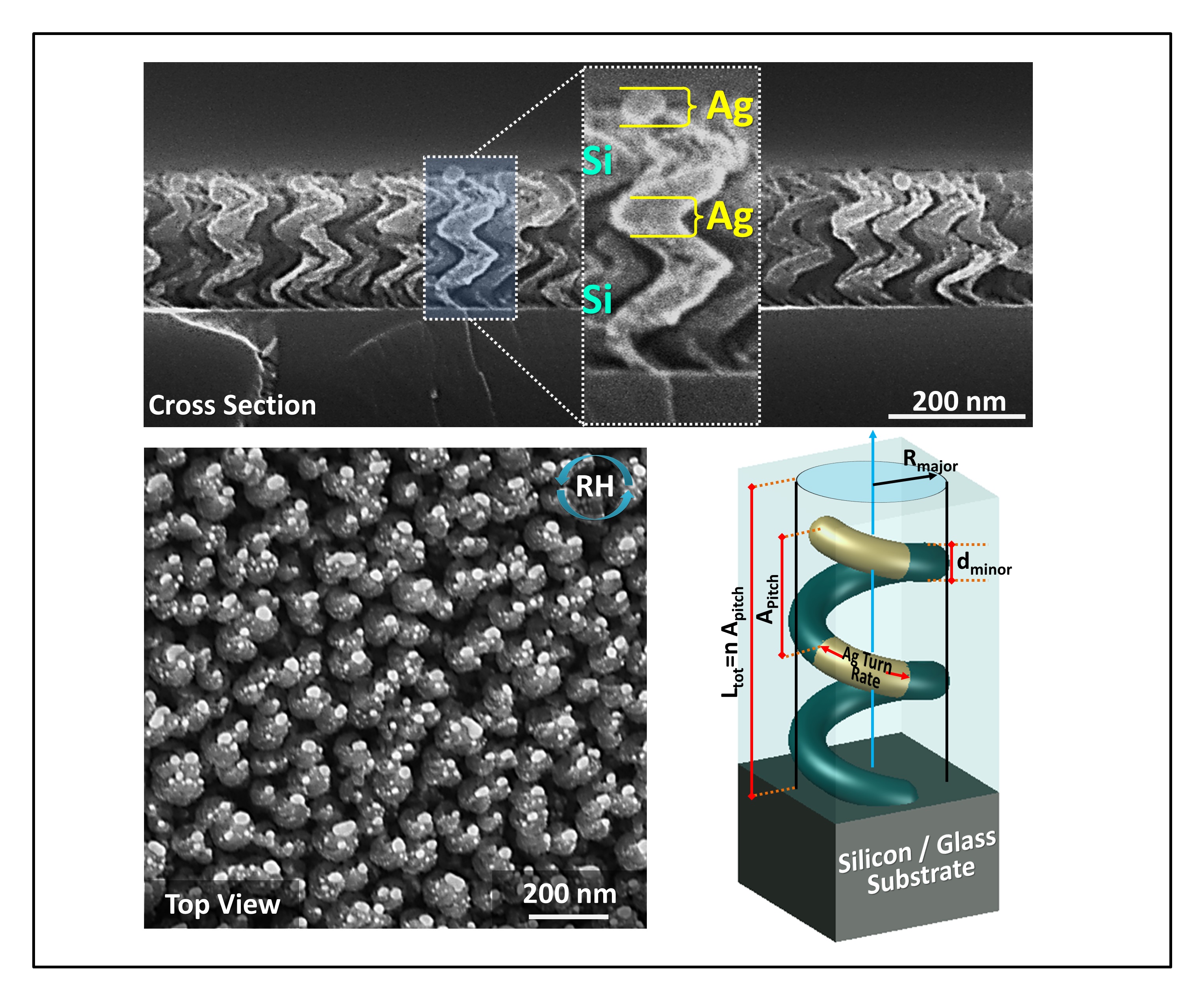
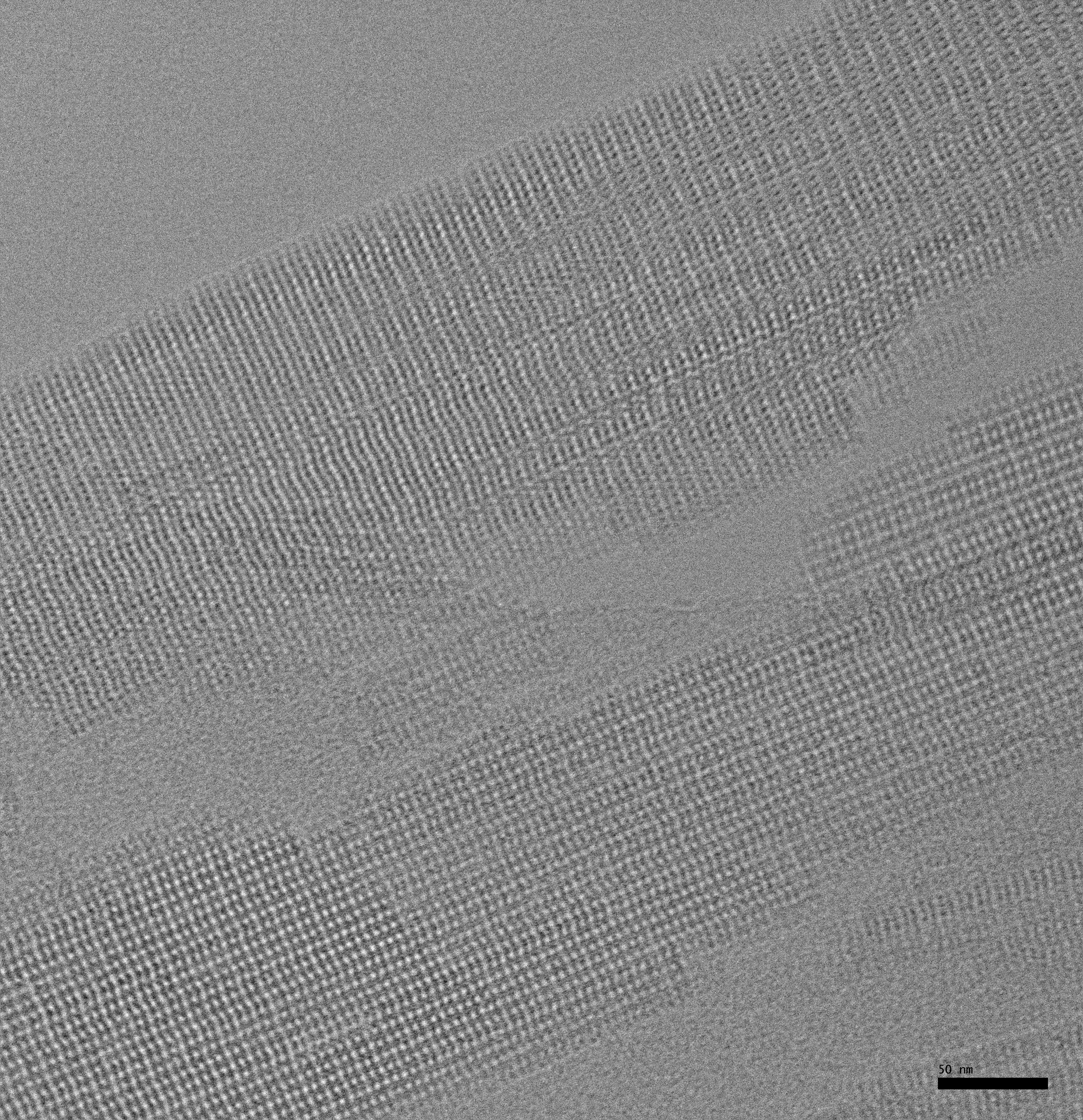
SiAg Chiral Nanoplasmonic Metasurfaces
Artists: Ufuk Kilic and Mathew Hilfiker, PhD. Students in Department of Electrical and Computer Engineering, Univ. of Nebraska-Lincoln
NNCI Site: NNF
Tool: The Helios NanoLab™ 660
Periodic nanoplasmonic structures offer extensive control of light–matter interactions and has recently gained great interest due to their potential usage in optoelectronic and photovoltaic devices, magnetic recording, microscopy, spectroscopy, and sensor applications. The highly porous, super lattice type, periodic arrangements of nano-plasmonic Silicon (Si)-Silver(Ag) chiral heterostructure thin films were fabricated by means of subsequent and repeated electron-beam glancing angle deposition from Si and Ag sources. In the Figure, high resolution cross section and top view Scanning Electron Microscopy images are shown together with the schematic illustration of an isolated single SiAg chiral heterostructure metasurface.
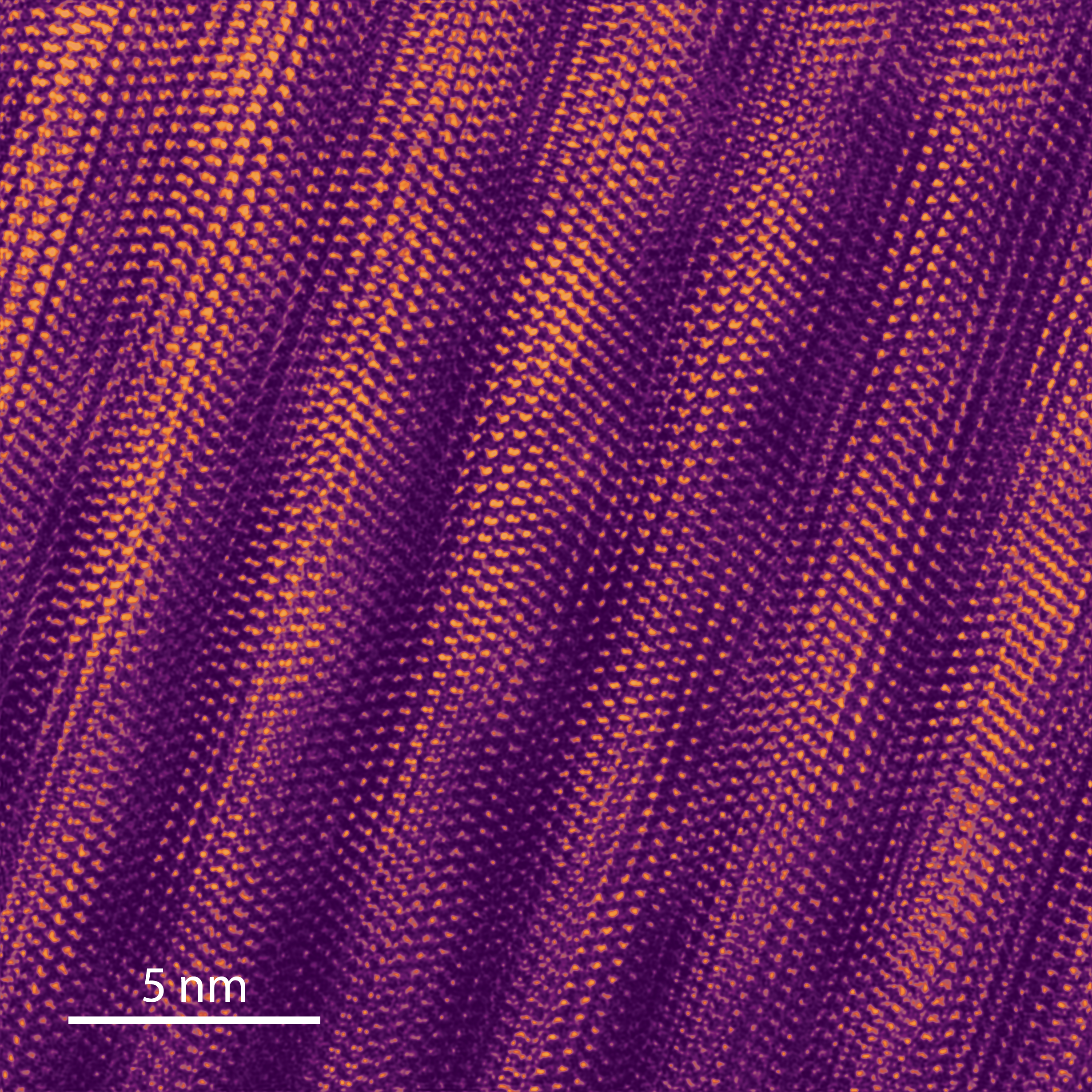
Kaleidoscope Eyes
Artist: Paul Smeets, NUANCE TEM Manager/Research Associate, Northwestern University
NNCI Site: SHyNE
Tool: JEOL ARM300F GrandARM TEM
Chiton are a type of marine organisms that use lenses embedded in their shell to focus light onto photoreceptors. Because their lenses - composed of the mineral aragonite - are birefringent, the micro- and nanostructure of the lens greatly impacts the optical performance. An ensemble of large, twinned grains and nanotwins ensures that the aragonite crystallographic c-axis is consistent across the lens, which in turn aids in limiting birefringence-induced aberrations. An example of multiple nanotwins close in proximity to each another (purple bands) are shown in this high-resolution transmission electron microscopy image, which additionally displays the atoms of the aragonite (orange). Beauty is in the eye of the beholder!
Microcrystalline Assembly State of Rubisco Activase (So Rca (66-359))
Artists: Isabella Breen, Graduate Student, and Rebekka Wachter, Professor, School of Molecular Sciences, Arizona State University
NNCI Site: NCI-SW
Tool: Titan Krios (FEI)
The enzyme responsible for atmospheric CO2 uptake and fixation is Ribulose-1,5-bisphosphate carboxylase/oxygenase, more commonly known as Rubisco. When Rubisco binds inhibitory sugar phosphates, it becomes inactivated and unable to catalyze the first major step of carbon fixation. An additional protein, rubisco activase (Rca), removes the inhibitor from the activation site and allows activity to continue. Recent evidence suggests that activase exists in many different higher-order assemblages that regulate the activity of Rca and therefore the rate of carbon fixation. Pictured is one of the 3 unprecedented arrangements so far observed via cryogenic transmission electron microscopy. With our research, we seek to understand the connection between these assemblies and the self-regulation of this life-sustaining protein. Scale bar: 50 nm
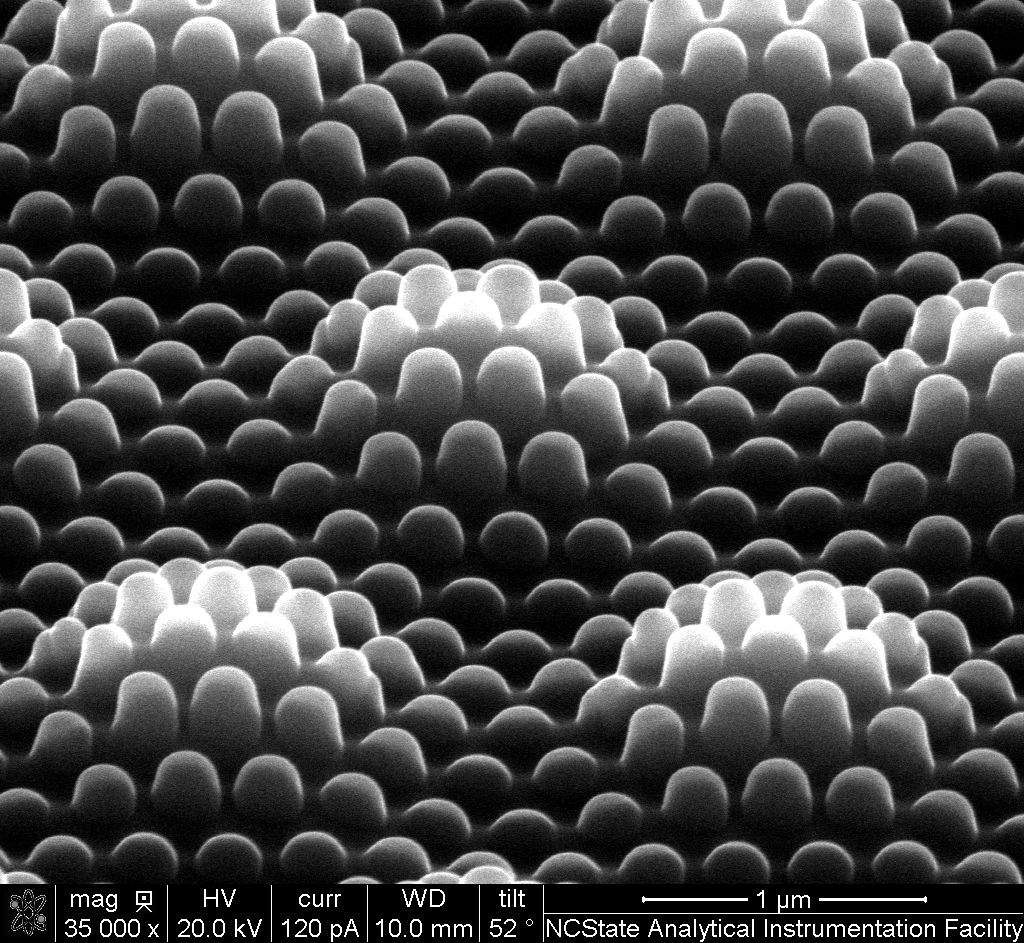
Nanocoined Structures in Diamond
Artists: Nichole Miller, Senior Scientist, Smart Material Solutions, Inc.
NNCI Site: RTNN
Tool: FEI Quanta 3D DualBeam FIB/SEM
This image shows hierarchical features that were milled into diamond using a focused ion beam (FIB). This nanopatterned diamond can be used as an indenting tool in the patented nanocoining process, which seamlessly nanopatterns cylindrical molds for roll-to-roll manufacturing hundreds of times faster than competing technologies. Nanocoining’s exceptionally high coverage rate enables the transfer of exciting lab-scale demonstrations of advanced optical and wetting properties to industrial-scale manufacturing for the first time.
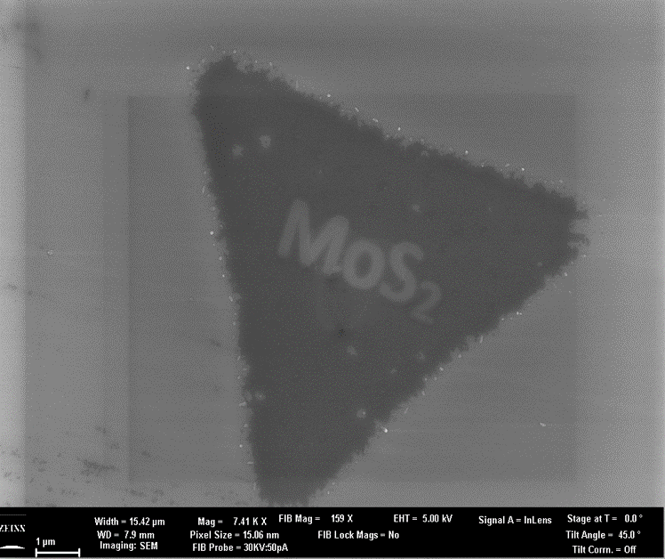
Helium Ion Calligraphy on 2D MoS2
Artist: Frederick Aryeetey, Graduate Student, and Kyle Nowlin, Research Associate, Nanoengineering, North Carolina A&T State University
NNCI Site: SENIC
Tool: Zeiss Orion Plus Helium Ion Microscope and Zeiss Auriga FIBFESEM
The electron micrograph shows precise patterns on two-dimensional Molybdenum disulfide (MoS2) monolayer created using 30 keV helium ions on a Zeiss Orion Plus Helium Ion Microscope. Imaging was done using the in lens detector on Zeiss Auriga FESEM. By controlling the pattern configuration and helium beam dose, it is possible to fabricate sub-10 nm features directly on single-layer MoS2. Introduction of defects through helium ion bombardment also can modulate the electronic and optical properties of layered materials such as MoS2.
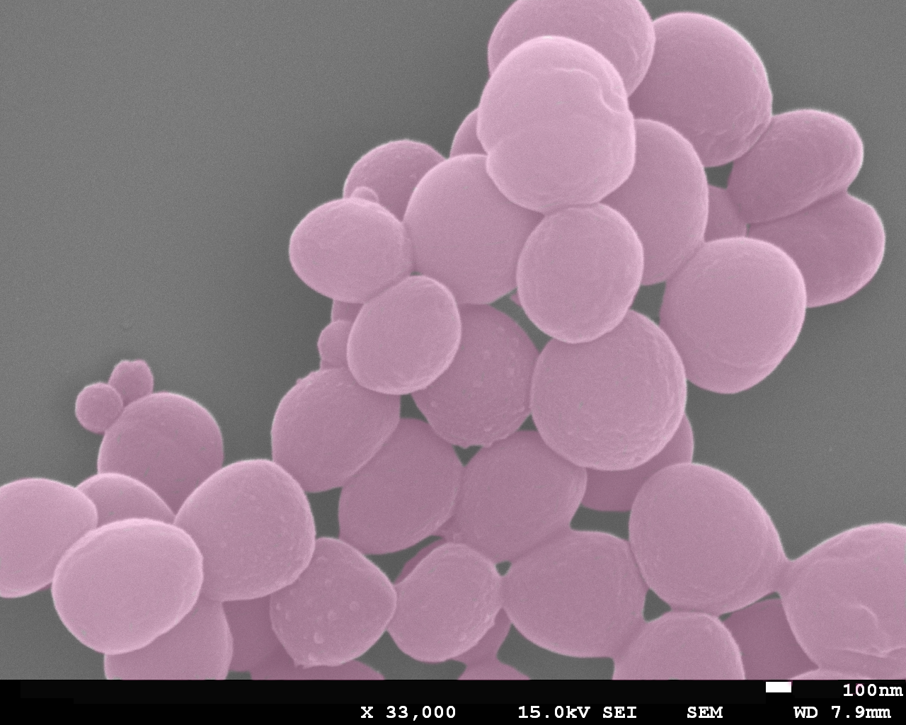
Healthy Staphylococcus aureus
Artist: Celine Burel, Senior Research Scientist at Solvay, COMPASS (a Solvay/UPenn/CNRS collaboration)
NNCI Site: MANTH
Tool: JEOL 7500F HRSEM
Quaternary ammonium compounds (QACs) are among the most commonly used disinfectants. QACs operate via disruption of one of the most fundamental structures in bacteria – the cell membrane – leading to cell lysis and bacterial death. The bactericidal efficacy of QACs is linked to their chemical structure and their membrane activity. The morphological membrane features of Gram-positive Staphylococcus aureus were studied with scanning electron microscopy. In a healthy state this 700 nm round bacteria present a smooth and intact cell wall without structural damage such as lysis, blisters or craters.
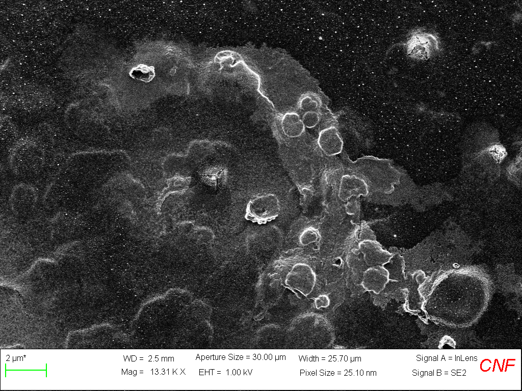
Death Star
Artist: Chris Martin, PhD, Ithaca Research Lab L.L.C.
NNCI Site: CNF
Tool: Zeiss SEM
Trapped gas dissolved in a furnace film process that ruptured during the densification anneal. Imaged on the Ultra at CNF.
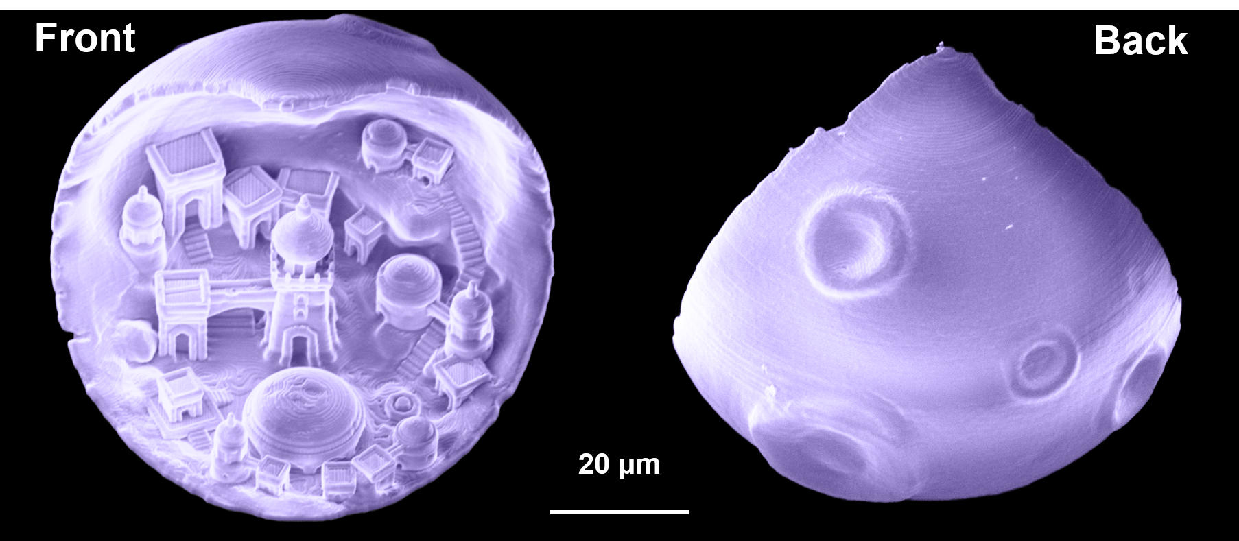
Moon City in the Nano Universe
Artist: Sarah K Lami, graduate student in Electrical and Computer Engineering, University of Kentucky
NNCI Site: KY Multiscale
Tool: Nanoscribe 3D Printing Technology
Moon City’s sculpture was fabricated at the KY Multiscale NNCI site using Nanoscribe 3d printing technology. “Shoot for the moon. Even if you miss, you’ll land among the stars.” – Les Brown
Original 3D model: Moon City by kijai, licensed under the Creative Commons - Attribution - Non-Commercial - No Derivatives license (CC BY-NC-ND 3.0)
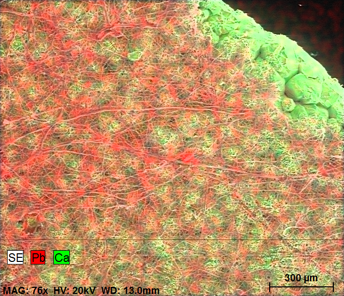
PoSH Eggshell
Artists: Anna Maria Petkoska, Yahya Kemal High School, Skopje, Macedonia, and Anita Trajkovska-Broach, CSI: Create. Solve. Innovate. LLC, Blacksburg, VA
NNCI Site: NanoEarth
Tool: FEI Quanta 600 FEG Environmental SEM
SEM EDS map of an eggshell with membrane taken within the PoSH™ (Porous Shells and Husks) project, which screens agricultural waste and industrial byproducts for their potential use as low-cost sorbents for environmental pollutants (e.g. heavy metals). The image shows lead (Pb) adsorbed on the egg membrane, when eggshells with membrane were immersed in Pb-contaminated water for 1 hr. These images were taken using the low-vacuum mode on the FEI Quanta 600 FEG Environmental SEM. By using low-vac mode the sample could be analyzed un-coated, in it's natural state, thus avoiding artifacts caused by sample coating and by exposure to high vacuum. Also beam sensitive samples, such as eggshells, can exhibit less electron beam damage in low vac mode.
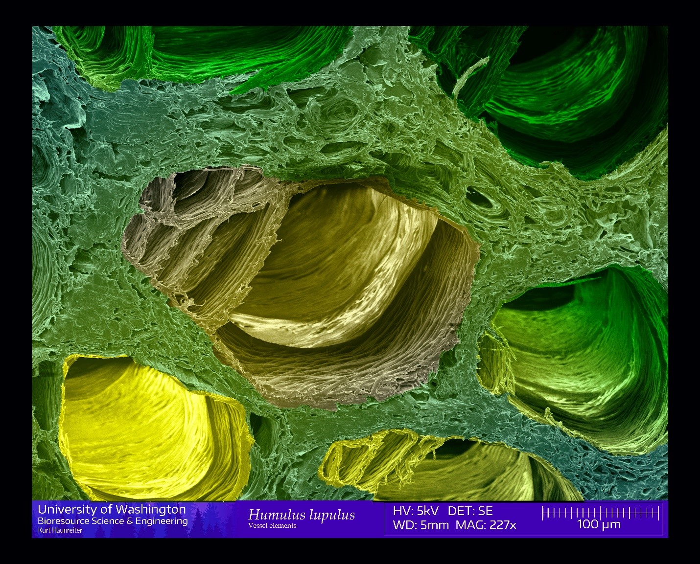
Humulus lupulus – Bine cross section - Vessel Elements
Artists: Kurt Haunreiter, Manager, Wollenberg Paper and Bioresource Science Laboratory, School of Environmental and Forest Sciences, University of Washington
NNCI Site: NNI
Tool: XL 30 SEM
This is a cross section of a hop bine showing the numerous vessel element structures in the woody plant. I am investigating an environmentally friendly oxidation method for breaking the cellulose into nano-cellulose. This examination is to document the morphological features present.
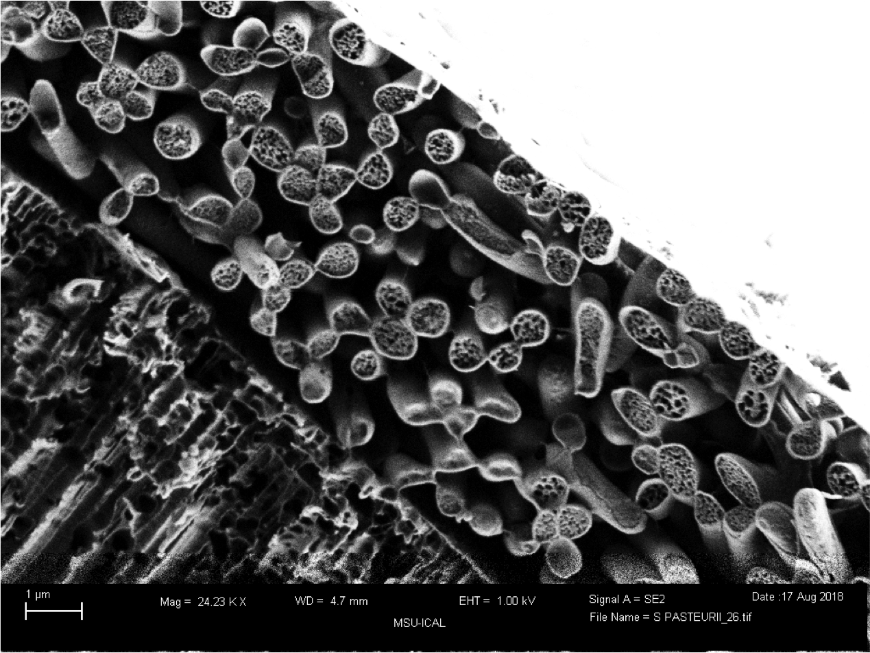
Fractured Biofilm
Artists: Adie Philips, PhD, and Kevin Hammonds, PhD, Montana State University
NNCI Site: MONT
Tool: cryo-stage equipped Zeiss FE-SEM
This image is of the cross section of a Sporosarcina pasteurii biofilm grown on a filter, immersed in liquid nitrogen and fractured so as to visualize it’s profile in depth with the cryo-stage equipped Zeiss FE-SEM in MSU’s ICAL. The image was taken by Adie Phillips and the methods to prepare the samples were developed by Adie Phillip and Kevin Hammonds. The purchase of the cryo-stage for the FE-SEM was supported by the 2017-2018 MSU NACOE Thorson Excellence in Engineering Research Grant.
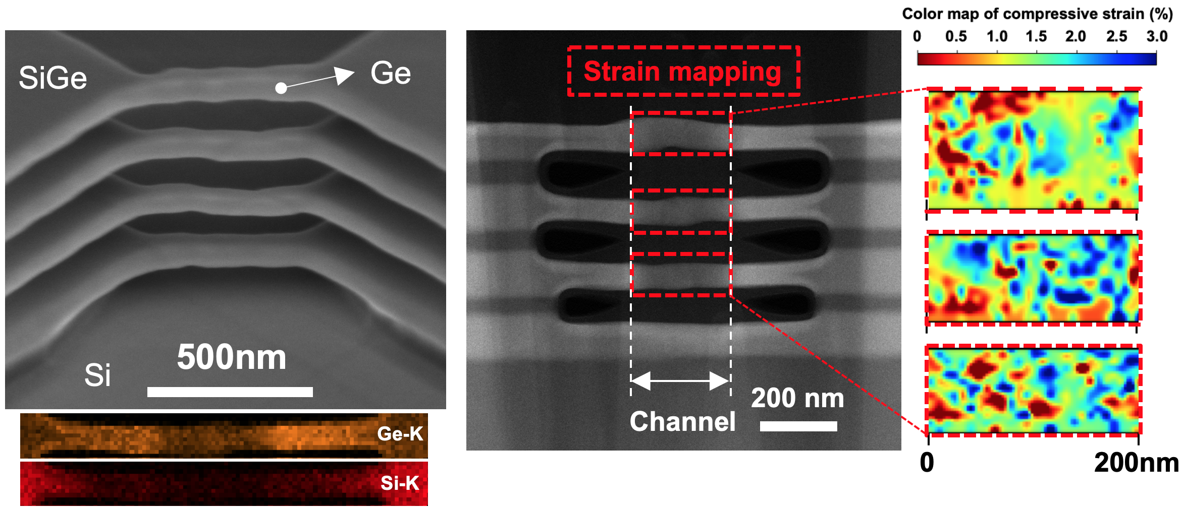
3D stacked suspended Ge nanowires on Si bulk
Artist: Junkyo Suh, PhD candidate, Electrical Engineering, Stanford University
NNCI Site: nano@Stanford
Tool: Helios SEM and Titan TEM
This is an image of vertically stacked Ge nanowires (NWs) on Si substrate. The structure is fabricated by growing SiGe epitaxial layers followed by Ge enrichment to create suspended Ge NWs (CMOS compatible technology). The device architecture is very promising for not only nano-electronics but also nano-photonics. 4D STEM (this is a new and unique technique that we have at Stanford) is performed to analyze strain accumulated in the Ge NWs (Diffraction pattern of Ge NWs in comparison with that of Si bulk).
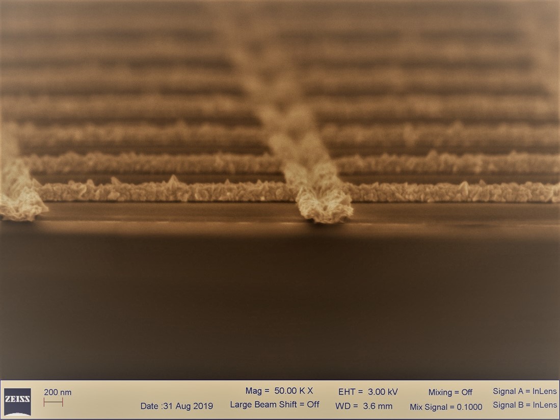
Cross Section of Selective Cu Metallization
Artist: Ziam Ghaznavi, graduate student, University of Texas at Austin
NNCI Site: TNF
Tool: Ziess Neon 40
The photo shows a cross section of selective Cu metallization using a roll-to-roll compatible fabrication process to make metal mesh based transparent conducting electrodes for optoelectronic device applications such as displays, lighting and electrochromics. The features in the image are roughly 300nm wide and 100nm in height.